CBSE Class 12 Physics Chapter 14 Revision Notes
Chapter 14: Semiconductor Electronic: Material, Devices And Simple Circuits Revision Notes
- Metals: They have extremely low resistivity or extremely high conductivity.
ρ ~ 10-2.10-8 Ωm, σ ~102. 108 Sm-1
- Semiconductors: Semiconductors have resistivity or conductivity intermediate between metals and insulators.
ρ ~ 10-5. 106 Ωm, σ ~ 10+5 .10-6 Sm-1
- Semiconductors come in a variety of shapes and sizes. The following are examples of semiconductors:
(i) Elements Semiconductor: These semiconductors, such as silicon and germanium, are available in their natural state.
(ii) Compound Semiconductors: CdS, GaAs, CdSe, InP, anthracene, polyaniline, and other metal compounds are used to make these semiconductors.
- Insulators: They either have a high or low conductivity.
ρ ~ 1011 . 1019 Ωm, σ ~ 10-11. 10-19 Sm-1
- Energy Band: The valence electrons of one atom are shared by more than one atom in a crystal due to interatomic interaction. The energy level is now split in half. An energy band is a collection of these closely spaced energy levels.
- Valence Band: The valence band is an energy band that includes the valence electrons’ energy levels.
- Conduction Band: The energy band above the valence band is known as the conduction band.
- Energy Band Gap: The energy band gap is the minimum energy required to shift electrons from the valence band to the conduction band (Eg ).
- The following are the energy band differences between a conductor, an insulator, and a semiconductor:
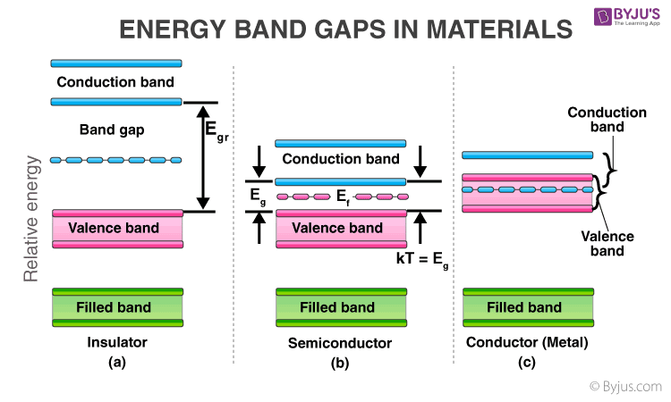
- Fermi Energy: At absolute zero temperature, it is the maximum possible energy possessed by free electrons in a material (i.e. 0K)
- Semiconductors are classified into two groups based on their purity:
(i) Intrinsic Semiconductors
It’s a pure semiconductor with no significant dopant species ne = nh =ni,
where ne and nh are the number densities of electrons and holes, respectively, and ni is the intrinsic carrier concentration.
An undoped semiconductor, also known as an i-type semiconductor, is an intrinsic semiconductor.
(ii) Extrinsic Semiconductors: Extrinsic semiconductor refers to a pure semiconductor that has been doped with an impurity.
There are two types of extrinsic semiconductors:
a) n-type semiconductors
b) p-type semiconductors
- Both types of semiconductors have the same electrical properties.
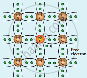
- In an n-type semiconductor, electrons make up the majority of charge carriers, while holes make up the minority, i.e. ne> nh.
- When we dope Si or Ge with a pentavalent element, four of its electrons bond with its four silicon neighbors, while the fifth is only weakly bound to its parent atom.
- The following diagram depicts the formation of an n-type semiconductor:
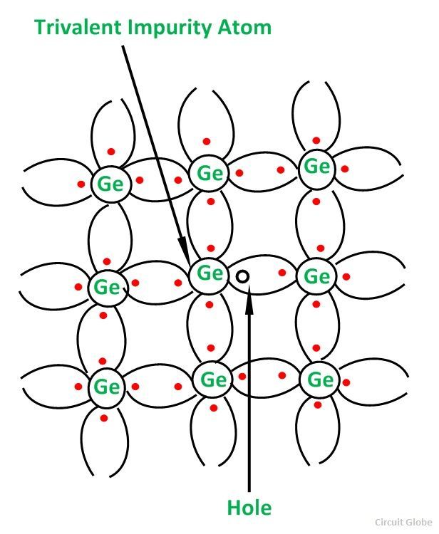
- In a p-type semiconductor, holes make up the majority of charge carriers, while electrons make up the minority, i.e. nh > ne.
- Doping is done in a p-type semiconductor with trivalent impurity atoms, which have three valence electrons in their valence shell.
- The following diagram depicts the formation of a p-type semiconductor:
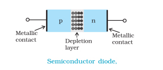
- p-n Intersection: A p-n junction is a semiconductor arrangement in which n-type and p-type semiconductors are in close contact.
- Depletion Region Formation in the p-n Junction: Due to the concentration gradient across the p and n sides, holes diffuse from the p-side to the n-side (p —> n) and electrons diffuse from the n-side to the p-side (n —> p) during the formation of a p-n junction.
- Depletion region refers to the space charge region on both sides of the junction.
- Mobile charge carriers are not present in the depletion region. The depletion region’s width is on the order of 10-6 meters. The potential barrier is the potential difference that has developed across the depletion region.
- P-n Junction Diode/Semiconductor Diode: A semiconductor diode is essentially a p-n junction with metallic contacts at the ends that allow an external voltage to be applied.
- The I-V characteristics of a junction diode are the graphical relationships between the voltage applied across the p-n junction and the current flowing through the junction.
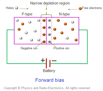
- When the positive terminal of the external battery is connected less to the p-side and the negative terminal to the n-side of the diode, the junction diode is said to be forward biased. A forward biased diode’s circuit diagram and I-V characteristics are shown below:
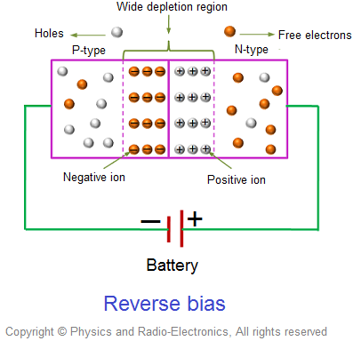
- A reverse biased diode’s circuit diagram and I-V characteristics are shown below.
- rDC = V/I is the DC resistance of a junction diode.
- rAC = V/I is the dynamic resistance of a junction diode.
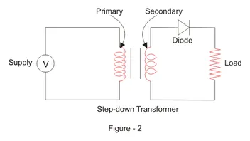
- Diode as Rectifier: Rectification is the process of converting alternating voltage/current to direct voltage/current. A rectifier is a device that converts alternating current and voltage into direct current and voltage.
(i) Diode as Half-Wave Rectifier: The diode conducts during the positive half of the cycle and does not conduct during the negative half. As a result, the diode converts AC to unidirectional pulsating DC. Half-wave rectification is the term for this process.
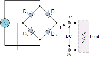
(ii) Diode as Full-Wave Rectifier: Two p-n junction diodes, D1 and D2, are used in the full-wave rectifier.
- Its operation is based on the principle that junction diodes have very low forward bias resistance and very high reverse bias resistance.
- A half-wave rectifier’s pulse frequency is equal to the frequency of AC.
- A full-wave rectifier’s pulse frequency is twice that of an AC source.
- Optoelectronic devices are semiconductor diodes in which the carriers are generated by photons, i.e. photo-excitation.
The following are some of them:
(i) Light Emitting Diode (LED): A LED is a highly doped p-n junction diode that converts electrical energy into light energy.
LEDs have the following advantages over traditional low-power incandescent lamps:
a) Quick action with no warm-up time;
b) Nearly monochromatic;
c) Low operational voltage and lower power consumption;
d) Fast ON-OFF switching capability.
(ii) Photodiode: A photodiode is a type of junction diode that is used to detect light signals. A photosensitive material is used to create a reverse biased p-n junction.
When reverse bias is applied, the current in the photodiode changes with the change in light intensity.
(iii) Photovoltaic Cell: A solar cell is a p-n junction diode that converts sunlight into electricity. Si and GaAs are the materials used in solar cells.
]]>